Laboratory of Semiconductor Characterization
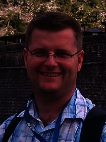
Piotr Kruszewski

dr Piotr Kruszewski
Interests: Electrical characterization of wide bandgap semiconductors (mostly GaN-based materials) and defects analysis by capacitance-based techniques: capacitance-voltage (C-V) in wide range of temperature (77K-700K), temperature dependent current-voltage (I-V), DLTS (Deep Level Transient Spectroscopy) and Laplace DLTS for defect characterization, SiPDR (Single Post Dielectric Resonator) – contactless and on-wafer/structure resistivity analysis, temperature-dependent Hall effect analysis, Hg-probe for non-destructive material analysis, Most structures and devices can be characterized on wafer by the 4-needle probe station (300K only)
Projects: SchottGan, Sonata Bis (NCN), PioneerGaN
Contact:
My phone number: + 48 22 876 04 42 (office), +48 22 876 04 40 (laboratory)
E-mail: kruszew(at)unipress.waw.pl