Laboratory of Semiconductor Characterization
Head of the Laboratory
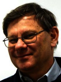
prof. Mike Leszczyński Born 1956 Academic: MSci 1980 Physics Dept of Warsaw University (X-ray topography of Si crystals after high pressure treatment). PhD 1990 Institute of Physics Polish Academy of Science (Lattice parameters of III-V compounds as a function of temperature and illumination) Habilitation 1996 Institute of Physics Polish Academy of Sciences (Microstructure of III-N compounds) Professor of Polish Academy of Sciences 2004. Professional experience: 1980- up to now, Institute of High Pressure Physics UNIPRESS, 1990-92- post-doc at Intitute of Theoretical Physics Trieste (Italy) and at Institute of Advanced Materials Brindisi (Italy) 1996- visiting professor at Center of Atomic Energy (CEA) Grenoble (France) 1997-2005- advisor for Philips Analytical 2001-up to now, vice president of TopGaN, spin off from Unipress, responsible for R&D activity. Publications: More than 350 paper published, cited more than 5000 times, Hirsch factor 30-34 (depending on source), 30 invited talks at international conferences. Scientific activity: 1980-1994: X-ray Diffraction (XRD) examinations of defects in GaAs, InP and GaN semiconductors. The main results of that period: i) observation of metastability of EL2-like defects (Ga-antisite in complex defect) induced by temperature and illumination, ii) determination of lattice parameters of GaAs and GaN as a function of doping. 1995-2000: creation of the epitaxy (metalorganic chemical vapour phase epitaxy-MOVPE) laboratory in Unipress, 2000- up to now: examinations of microstructural properties of AlGaInN layers and quantum structures as a function of MOVPE growth conditions and relating these properties to the optical and electrical parameters which are important for functioning of nitride laser diodes (UV/blue/green) and transistors. Commercial activity: In 2003, two years after TopGaN had been founded, I joined this spin-off as a vice-president responsible for R&D activity. Till now, most of the efforts of TopGaN has been devoted to R&D because of three reasons: i) company was founded at a very early stage of technology (no epitaxy, no processing), ii) nitride technology turned out to be much more difficult as had been expected, iii) most of TopGaN products (laser diodes and epi wafers) are being developed and customized for new products of our customers. Recently, TopGaN spun-off a new company TopGaN Quantum Technology (in Glasgow) in order to participate in the production of new generations of atomic clocks. At the same time, TopGaN was invited by the largest car-headlamp producer Valeo to participate in the development of smart headlights based on TopGaN’s addressable laser arrays. Grants received: Leader of 16 grants awarded by the agencies in Poland, Examples: Single-mode and high-power laser diodes based on gallium nitride, POIG (Operational Program Innovation Economy, 2008-11 Ultraviolet (380 nm) laser diodes for spectroscopic applications, National Research and Development Center (NCBiR), INNOTECH, 2011-14 Optimisation of GaN and SiC off-orientation for electronic devices, POIG (Operational Program Innovation Economy, 2013-1 New method of fabrication of InGaN/GaN quantum wires, Project of National Science Center (NCN), 2016-18 New generations of InGaN layers, quantum wells and wires grown on vicinal GaN substrates for optoelectronics and photovoltaics, V4-Japan Project, 2015-18 Leader of workpackages in 18 grants awarded by the Commission of the European Union. Examples: Project acronym: NEWLED, Integrated Project of VII EU Framework Project full title: "Nanostructured Efficient White LEDs based on short-period superlattices and quantum dots" Project title SHYMAN—Sustainable Hydrothermal Manufacturing of Nanomaterials Call (part) identifier FP7-NMP-2011-LARGE-5, 2013-16 Project acronym: NANOTEC Project full title: Nanostructured materials and RF-MEMS RFIC/MMIC technologies for highly adaptive and reliable RF systems Grant agreement no.: FP7-ICT-2011-7 2013-15 Professional Memberships: Leader of Thin Film Group in the Polish Society of Crystal Growth Member of the following committees of International Conferences: International Conference on Nitride Semiconductors ICNS-every 2 years (about 2000 participants) International Conference on White LEDs and Solid State Lighting WLED- every 2 years (about 3000 participants) International Conference on Crystal Growth ICCG-every 3 years (about 1000 participants) International Conference on Metalorganic Chemical Vapour Phase Epitaxy ICMOVPE- every 2 years (about 600 participants) European Workshop on Metalorganic Chemical Vapour Phase Epitaxy EWMOVPE- every 2 years (about 200 participants) Expert Evaluation & Control of Compound Semiconductor Materials & Technologies EXMATEC- every 2 years (about 200 participants) Forum of New Materials CIMTEC, Montecatini (It), Workshop on Solid State Lighting- every 2 years (about 200 participants) Microtechnology and Thermal Problems in Electronics MICROTHERM, Łódź- every 2 years (about 100 participants). International collaboration According to Google Scholar, out of 360 of my publications, 113 have been published with the authors from France, Germany, USA, Japan, Italy, UK, Lithuania and Greece. In many cases, we just supplied unique samples of AlGaInN, and our coworkers examined them using various techniques. However, with some of the foreign labs we have a long-tradition collaboration, for example, with: Vilnus University (EU projects GaNano, NewLED) on optical characterization of AlGaIN epi wafers, University of Montpellier (bilateral France-Poland projects) on Teraherz emitters, CRHEA (France) (EU projects NEWLED, Granite) on epitaxial growth, University of Ulm (Germany) on epitaxial growth, IMM-CNR (Italy) (bilateral project ETNA, EU projects: Last Power, Granite) on GaN-based electronic devices, OPTOCAP (UK) (EU projects: GaNbar, Blucom and ESA projects) on atomic clocks and laser diode packaging. In particular, it is worth to mention the Japan-V4 project WISEGaN coordinated by me. This project is on new methods of quantum structure fabrication for blue optoelectronics. The partners in this consortium are Hiroshi Amano (Nagoya University- Nobel prize winner) and Vaclav Holy (Charles University- world expert on X-ray Diffraction). Other information i) Supervision of 7 PhD students, ii) 2006-2014: lectures for PhD students on crystal growth and characterization, iii) Reviewer for Journal of Crystal Growth, Applied Physics Letters, Physica Status Solidi, and others, iv) Reviewer 15 PhD dissertations in Poland, Lithuania and Greece. v) Reviewer about 100 grant proposals in Poland, Lithuania and the Czech Republic. vi) Leader of the Thin Film Group in the Polish Society of Crystal Growth.
Interests: Semiconductor technology, crystal growth, defects in crystals
Projects: V4-Japan Project WISEGAN, SchottGaN
Contact:
E-mail: mike@unipress.waw.pl